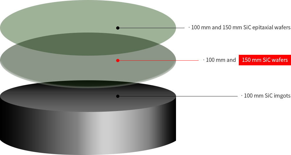
SiC Wafer
실리콘 카바이드 웨이퍼는 가혹한 조건에서 더 높은 성능을 요구하는 장치에 적합한 와이드 밴드 갭 반도체 재료입니다.
가장 대표적인 적용 분야로는 차세대 친환경 자동차와 재생 에너지 보급 설비입니다.

Prime 등급에 따른 적용분야
| Portfolio | Features & Benefits | Typical Applications |
|---|---|---|
| Prime Standard | Guaranteed MPD tolerances. Balances performance and cost for electronic components with low to medium current ratings. | Schottky and junction barrier Schottky diodes |
| Prime Select | More stringent tolerances for MPD current ratings and TSD. Allows for manufacturing with mid-range current ratings. |
Pin diodes and switches |
| Prime Ultra | Extremely low MPD, TSD and BPD tolerances and tightened wafer resistivity. Ensures product quality and improves cost efficiency in manufacturing high current devices. | High current and voltage MOSFETs, JFETs, IGBTs, BJTs and pin diodes with large die ares |
재료 특성
전체 속성 요약은 이하 제품 데이터 시트를 참조하십시오.
| Product metric | Standard | Select | Ultra |
|---|---|---|---|
| Diameter, mm | 14938 – 150.2 | ||
| Thickness, ㎛ | 325 – 375 | ||
| Primary flat length, mm | 45 – 50 | ||
| Bow, ㎛ | ± 30 | ||
| Warp, ㎛ | ≤ 50 | ||
| TTV, ㎛ | ≤ 10 | ||
| SBIR, ㎛ | ≤ 5 | ||
| Foreign polytypes, % | 0 | ||
| Visible scratches, mm | ≤ 40 | ||
| Resistivity, ohm-cm | 0.014 – 0.024 | 0.014 – 0.023 | 0.014 – 0.022 |
| Total usable area, % | ≥ 90 | ≥ 95 | ≥ 97 |
| Dislocation density, cm-2 | |||
| EPD (mean) | ≤ 15,000 | ≤ 12,000 | ≤ 9,000 |
| TED (mean) | ≤ 10,000 | ≤ 9,000 | ≤ 8,000 |
| TSD (mean) | ≤ 3,000 | ≤ 500 | ≤ 400 |
| BPD (mean) | ≤ 5,000 | ≤ 4,000 | ≤ 3,000 |
| MPD, cm-2 | ≤ 1 | ≤ 0.5 | ≤ 0.3 |

